Exclusive | Tech war: China quietly making progress on new techniques to cut reliance on advanced ASML lithography machines
- By applying SAQP to DUV machines, China could make sophisticated 5-nanometre grade chips without the need for more advanced EUV tools sold only by ASML
- Local semiconductor equipment leader Naura Technology Group began preliminary research into lithography systems in March, according to sources
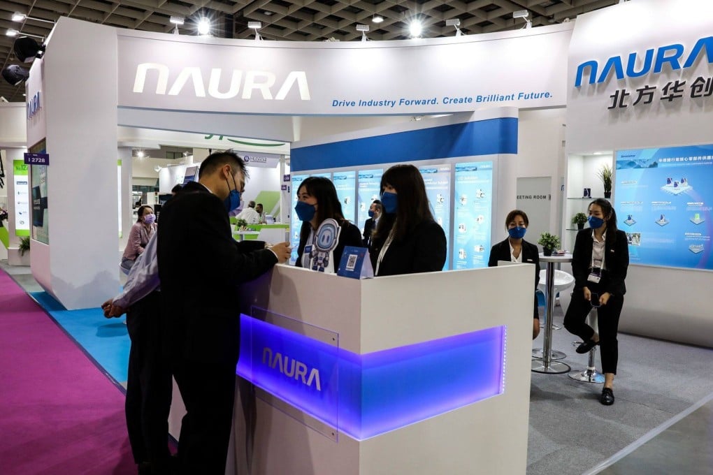
Beijing-based Naura Technology Group started research on lithography systems last month, according to people familiar with the matter, as China’s home-grown semiconductor tool makers try workarounds to produce advanced chips without the latest equipment from Dutch giant ASML, a breakthrough that could potentially thwart US attempts to contain China’s chip-making capabilities.
The efforts, which involve multiple players in China’s semiconductor supply chain, have made preliminary research progress, with a patent application by Huawei Technologies last month revealing a technique known as self-aligned quadruple patterning, or SAQP, which can etch lines on silicon wafers multiple times to increase transistor density and chip performance.
The patent, which combines advanced etching and lithography, “will increase the design freedom of circuit patterns”, according to a filing to the China National Intellectual Property Administration, which was first reported by Bloomberg.
By using SAQP with deep ultraviolet lithography (DUV) machines from Dutch giant ASML and Japanese suppliers like Nikon, China could make sophisticated 5-nanometre grade chips without the need for more advanced extreme ultraviolet (EUV) tools only available from ASML.