Advertisement
Chinese telecoms giant Huawei pushes semiconductor packaging innovation to ease disruptions caused by US chip sanctions
- Huawei has filed a patent application on the mainland for ‘a type of chip stacking package and terminal device’
- This innovation comes days after rotating chairman Guo Ping suggested that Huawei would use advanced chip packaging technology to help ease US restrictions
Reading Time:3 minutes
Why you can trust SCMP
1
Chinese telecommunications giant Huawei Technologies Co has filed a patent application on the mainland for a semiconductor packaging innovation, which industry analysts describe as a potential way to ease the disruptions caused by US chip sanctions on the firm’s operations.
The company’s patent application for “a type of chip stacking package and terminal device” is expected to help “solve the problem of high costs due to the use of through-chip via [also known as through-silicon via or TSV], while ensuring power supply requirements”, according to a statement released on Tuesday by the China National Intellectual Property Administration.
This innovation comes days after Huawei rotating chairman Guo Ping suggested at a press conference for the company’s annual report that it would use advanced chip packaging technology to help alleviate the firm’s struggles with US trade sanctions.
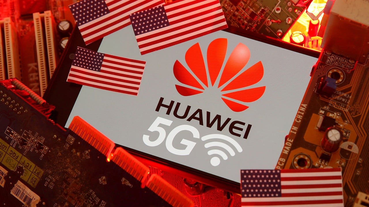
Privately-held Huawei, the world’s largest telecoms equipment maker and formerly China’s biggest smartphone vendor, was added to Washington’s trade blacklist in May 2019. The company has since scrambled to adapt its operations to tighter restrictions imposed in 2020, covering access to chips developed or produced using US technology, from anywhere.
05:22
Huawei founder on cybersecurity and maintaining key component supply chains under US sanctions
Huawei founder on cybersecurity and maintaining key component supply chains under US sanctions
Huawei did not immediately reply to a request for comment on Thursday.
TSV technology enables stacked chips to interconnect through direct contact, providing high-speed signal processing and improved photo detection for image sensing, according to a 2009 Institute of Electrical and Electronics Engineers paper. TSV was introduced into high-volume chip manufacturing during the past decade.
Advertisement