Could this way of making ultra-thin semiconductors lead to faster microchips?
- Research by Chinese team addresses key barrier to reducing the size of traditional silicon-based chips
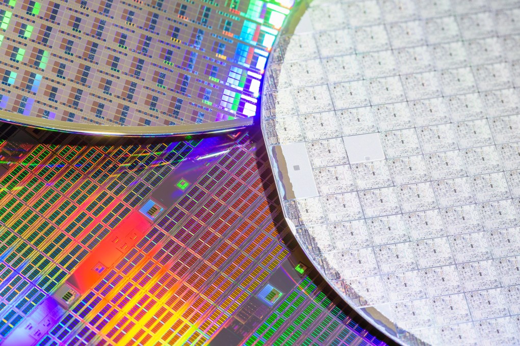
A team led by Liu Kaihui of Peking University, Liu Can of Renmin University, and Zhang Guangyu of the Institute of Physics at the Chinese Academy of Sciences developed a fabrication method to produce a semiconductor material just 0.7 nanometres thick.
The researchers’ findings, which were published in the peer-reviewed journal Science on July 5, address a key barrier to reducing the size of traditional silicon-based chips – as devices shrink, silicon chips run into physical limits that affect their performance.
The scientists explored two-dimensional (2D) transition-metal dichalcogenides (TMDs) as an alternative to silicon, with a thickness of just 0.7 nanometres compared to silicon’s typical 5-10 nanometres.
TMDs also consume less power and have superior electron transport properties, making them ideal for the ultra-scaled down transistors that will be a feature of next-generation electronic and photonic chips.
However, producing TMDs has been challenging – until now. According to the paper, the technique developed by the scientists allows them to quickly produce high-quality 2D crystals in seven formulations, making mass production feasible.
The traditional fabrication process, which involves layer-by-layer assembly of atoms on a substrate – like building a wall with bricks – often results in crystals with insufficient purity, Liu Kaihui told state news agency Xinhua.